
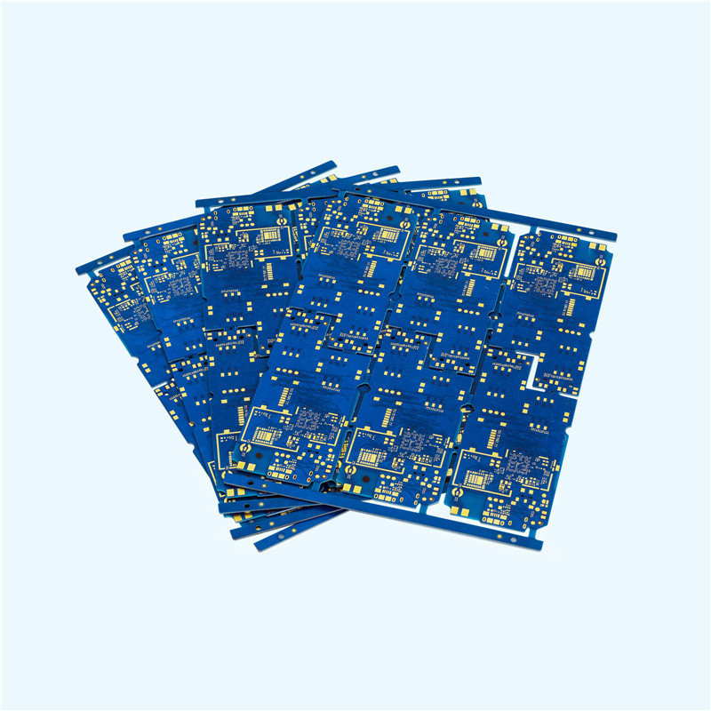
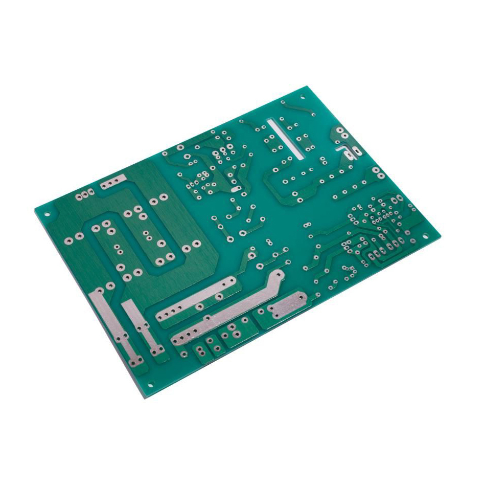
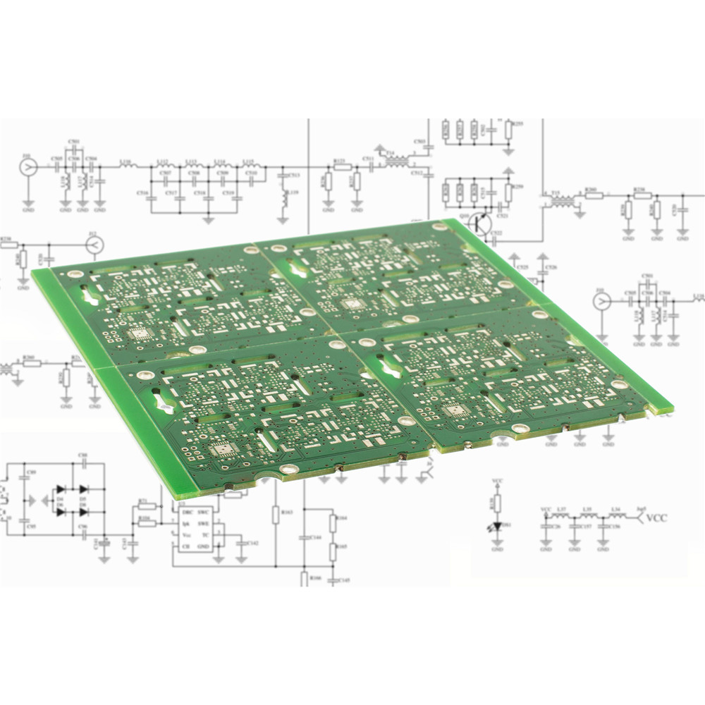
Multilayer Printed Circuit Boards
WHAT IS A MULTILAYER PCB?
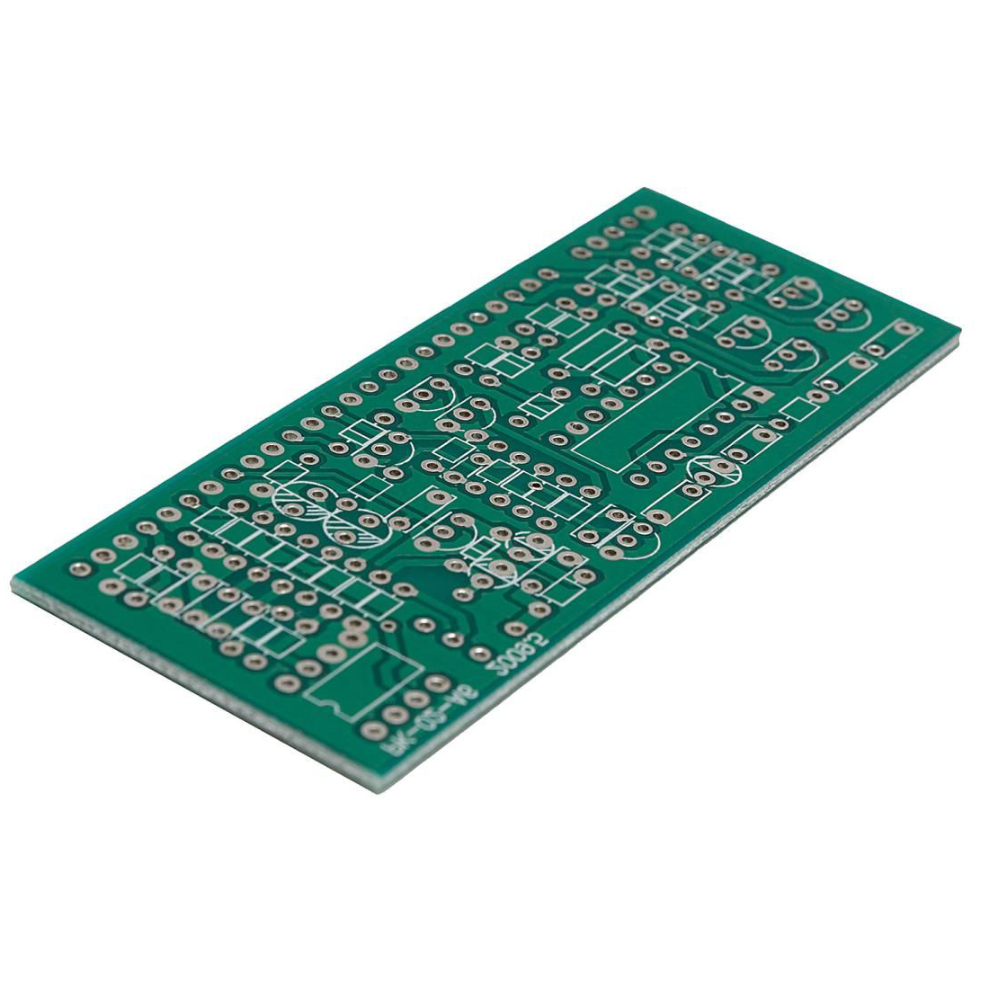
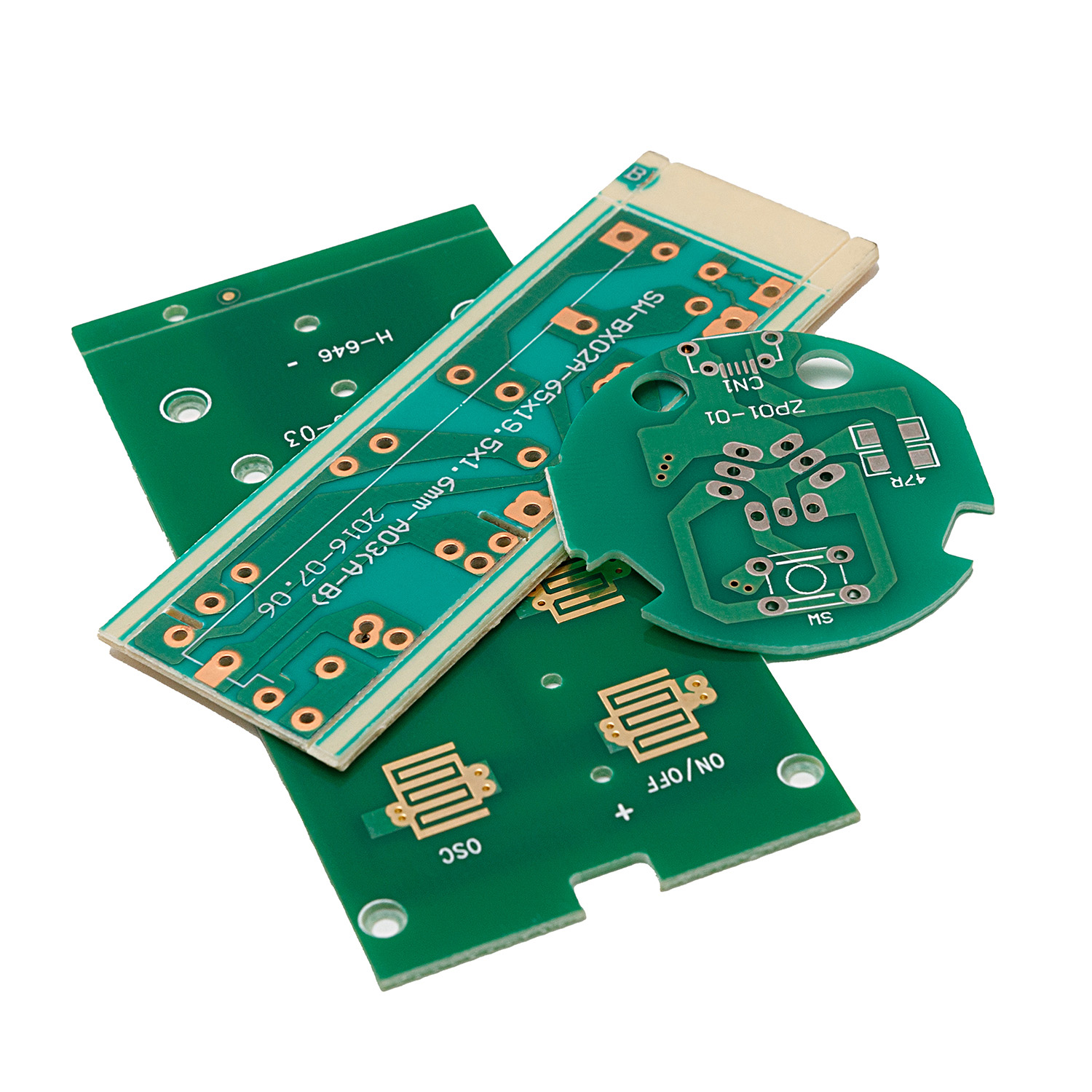
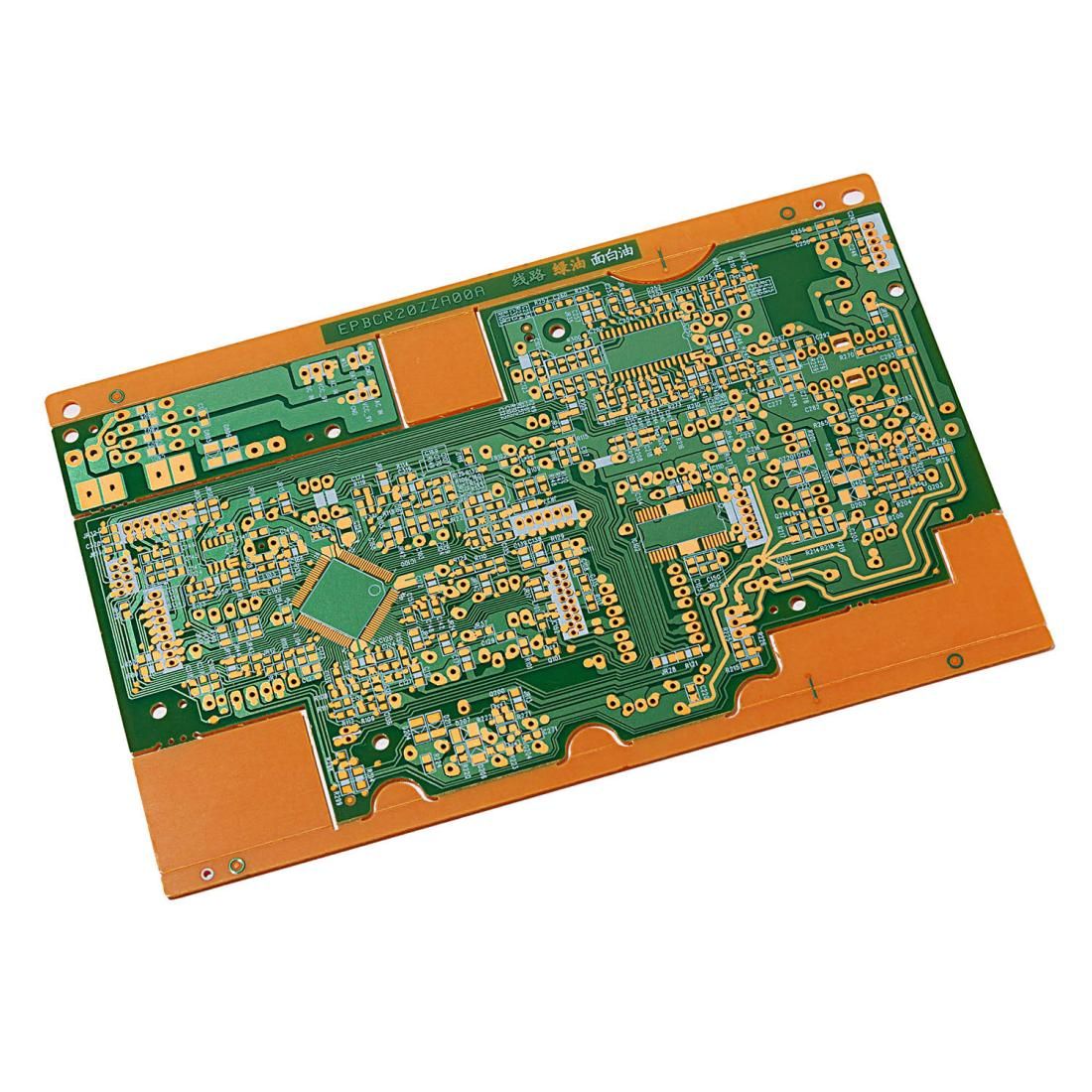
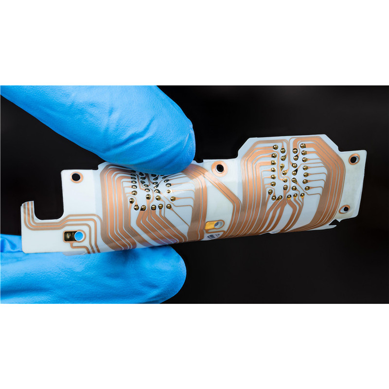
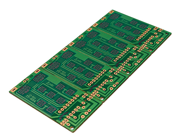 It is a PCB made with three or more conductive copper layers. The conductive foil appears to be various layers of a multi-sided circuit board. The different inner layers are processed in pairs (on a core) and then bonded together using prepreg as the insulating layer. The layers are then placed in such a way that both sides of the PCB can be used to mount components with additional tracking/electrical connections on the inside of the board. Vias are used as a source of the electrical connections between the different layers of a multilayer PCB.
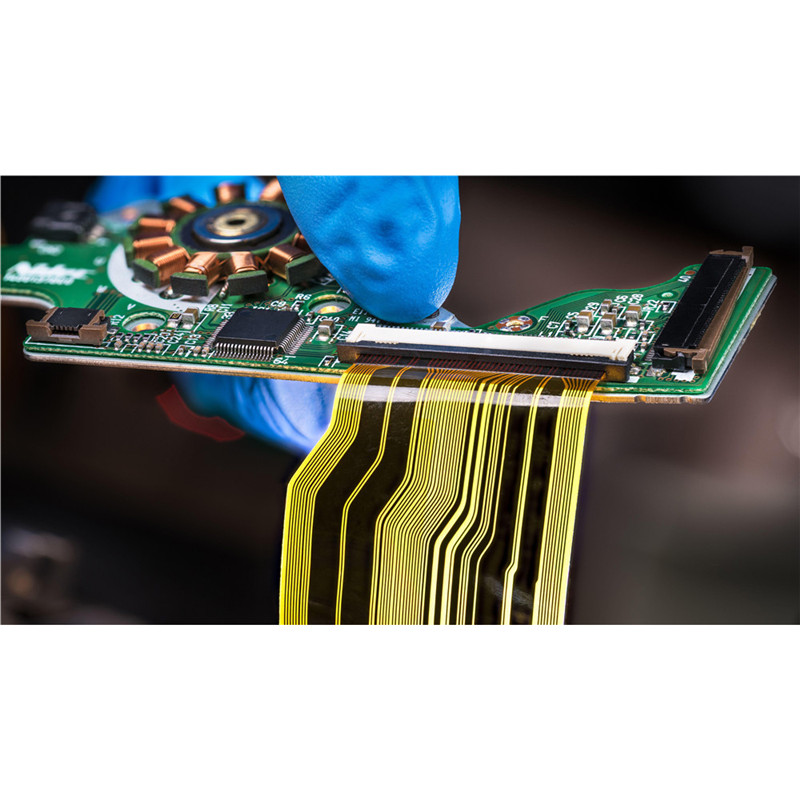
Many products use multilayer PCBs, including computers, medical equipment, in-car systems, GPS and satellite systems, industrial control systems.
Please contact us if you need further information or assistance, we are happy to help you.
Product Specifications
| Feature | AREX´s technical specification |
|---|---|
| Number of layers | 4 – 22 layers standard, 30 layers advanced, 40 layers prototype. |
| Technology highlights | Multiple layers of epoxy glass fiber bonded together with multiple layers of copper of varying thicknesses. |
| Materials | High performance FR4, halogen-free FR4, low loss and low Dk materials |
| Copper weights (finished) | 18μm – 210μm, advanced 1050μm / 30oz |
| Minimum track and gap | 0.075mm / 0.075mm |
| PCB thickness | 0.40mm – 7.0mm |
| Maxmimum dimensions |
580mm x 1080mm, advanced 610mm x 1400mm |
| Surface finishes available | HASL (SnPb), LF HASL (SnNiCu), OSP, ENIG, Immersion Tin, Immersion Silver, Electrolytic gold, Gold fingers |
| Minimum mechanical drill | 0.20mm |
| Minimum laser drill | 0.10mm standard, 0.075mm advanced |
Product service
Nothing affects the PCB’s cost and quality as much as the initial design. As modern electronic products are expected to offer more and more advanced functions, while the products themselves are becoming smaller and smaller, this puts greater demands on the PCB design and the importance of making the right choices at the design stage.
More than 30% of the Gerber data packs we receive do have some issues, generally, ambiguous information, errors, design rule conflicts, missing information and contradictions between the data and specifications. To prevent that it gets wrong from the start, we have put together these design guidelines, to use as a checklist.
When using combinations of parameters, you should always consult us to get the solution.